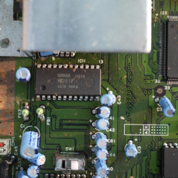
YM2612

The YM2612 (the smaller cousin of the YM2608) is the Sega Mega Drive's main sound chip. It is capable of outputting 6 channels of FM synthesis, meaning it can re-create almost any instrument you could think of by using some algorithms, which are specified by 'voices.' The chip can output stereo sound, which means a channel can be left, right, or both. To create accurate drums, snares, and more, many games trade the YM2612's 6th FM channel in for a DAC channel to play back these pre-recorded samples.
To access the YM2612, you write into a specific area of IO memory, which is often done by the Z80 when it runs the sound driver, or the M68k when it is running the sound driver.
If distortion of a channel is required, one can utilize the chip's LFO, or Low Frequency Oscillator. As mentioned earlier, the YM2612's 6th FM channel can be used as a DAC channel by the means of the 'DAC Enable' register on the chip. DAC data is written to an 8-bit register. The YM2612 does not provide any facilities to handle buffering, mixing, or timing of this data, so any timing and mixing will need to be done in software on either the Z80 or the M68k.
Yamaha removed the better 14-bit accumulator-equipped sound mixer and replaced it with an easier and presumably cheaper to manufacture time-division sound multiplexer, which first truncates the 14-bit output to 9 bits, and then rapidly loops through outputting all channels. This truncation causes a glitch as the wave form approaches zero, also known as the 'ladder effect.' To solve this, external filtering circuitry is used which distorts the sound even further. Sega used an improved YM2612 in the Model 2 Mega Drive which does not have this issue, but problems with the sound filtering circuit cause a more distorted sound. Sega also used this chip in a number of it's arcade game cabinets.
The chip is programmed through a number of 8-bit registers, some being stitched together to form longer registers, such as with the timers. In this case, the most significant byte is written first. The timers have to be constantly polled by software to yield a result, mainly due to the fact that they do not cause an interrupt for either of the two processors. The constant polling of timers may cause some inaccuracies to occur.
Contents
Registers
As stated before, the chip is programmed through a number of registers. Due to the large number of registers available, writing to the YM2612 is divided into two parts. Part 1 has it's own word-wide address, while part 2 has it's own separate word-write port.
Part 1
Below is a small map illustrating the arrangement of registers in Part 1:
| D7 | D6 | D5 | D4 | D3 | D2 | D1 | D0 | |
|---|---|---|---|---|---|---|---|---|
| 22H | LFO enable | LFO frequency | ||||||
| 24H | Timer A Most Significant Bits | |||||||
| 25H | Timer A Least Significant Bits | |||||||
| 26H | Timer B | |||||||
| 27H | Ch3 mode | Reset B | Reset A | Enable B | Enable A | Load B | Load A | |
| 28H | Operator | Channel | ||||||
| 29H | ||||||||
| 2AH | DAC | |||||||
| 2BH | DAC enanle | |||||||
| 30H+ | DT1 | MUL | ||||||
| 40H+ | TL | |||||||
| 50H+ | RS | AR | ||||||
| 60H+ | AM | D1R | ||||||
| 70H+ | D2R | |||||||
| 80H+ | D1L | RR | ||||||
| 90H+ | SSG-EG | |||||||
| A0H+ | Frequency number LSB | |||||||
| A4H+ | Block | Frequency Number MSB | ||||||
| A8H+ | Ch3 supplementary frequency number | |||||||
| ACH+ | Ch3 supplementary block | Ch3 supplementary frequency number | ||||||
| B0H+ | Feedback | Algorithm | ||||||
| B4H+ | L | R | AMS | FMS | ||||
These registers are programmed through 4000h-4001h on the Z80 side, or A04000h-A04001h from the M68k side. Note that the data bus to the YM2612 is only 8 bits.
Part 2
Part 2's memory map is mostly the same as the one above - except the channels 1-3 in Part 1 are channels 4-6 in Part 2. The registers are also programmed through 4002h-4003h on the Z80 side, or A04002h-A04003h from the M68k side.